Chemical etching & PCB photoengraving
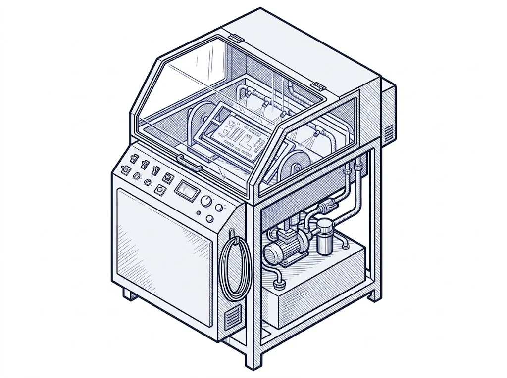
Chemical etching and PCB photoengraving are processes in which a corrosive reagent selectively removes material from the unprotected areas of a surface, leaving intact the geometry covered by a resist or a photo-hardening mask. In the production of printed circuit boards (PCBs), the standard process involves exposing a photoresist-coated board to the UV layout of the circuit, developing the resist, immersing the board in a ferric chloride or ammonium persulphate solution that dissolves the unprotected copper, then removing the remaining resist: the result is the conductive path of the circuit.
This technique is the backbone of hobbyist and professional electronic prototyping, making it possible to produce single- or double-sided circuits in the lab with track widths down to 0.3–0.5 mm. For art and jewellery, the same logic applies to acid etching of steel or brass using vinyl masks or resist paints to achieve permanent relief decorations.
Machines for this process
No sheets published here yet.
We're verifying the first machines for this process. In the meantime you can browse the whole catalog →